- 您现在的位置:买卖IC网 > Sheet目录2008 > MAX1394ETB+T (Maxim Integrated Products)IC ADC 8BIT 416KSPS 10-TDFN-EP
MAX1391/MAX1394
_______________________________________________________________________________________
3
1.5V to 3.6V, 416ksps, 1-Channel True-Differential/
2-Channel Single-Ended, 8-Bit, SAR ADCs
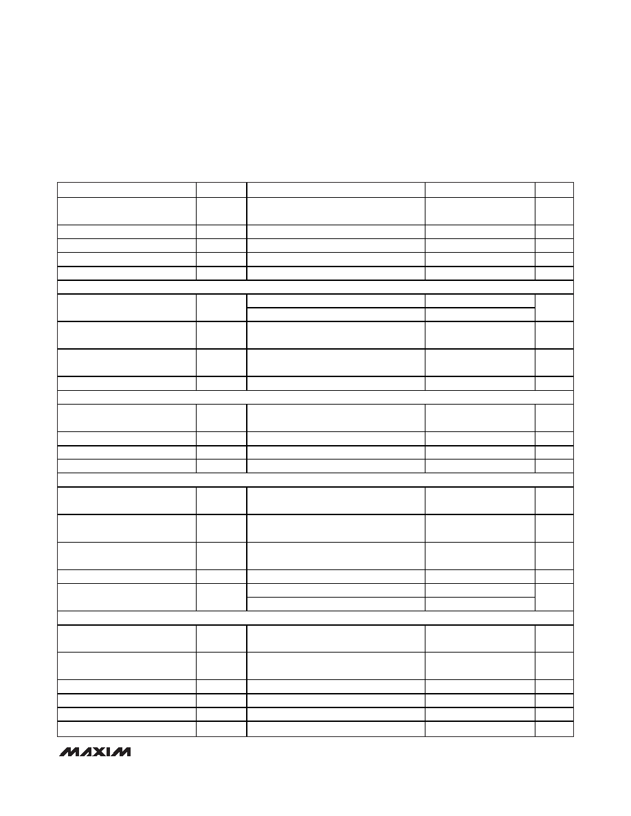
ELECTRICAL CHARACTERISTICS (continued)
(VDD = +1.5V to +3.6V, VREF = VDD, CREF = 0.1F, fSCLK = 5MHz, TA = TMIN to TMAX, unless otherwise noted. Typical values are at
TA = +25°C.) (Note 1)
PARAMETER
SYMBOL
CONDITIONS
MIN
TYP
MAX
UNITS
Throughput Rate
12 clocks per conversion, includes power-
up acquisiton and conversion time
416
ksps
Power-Up and Acquisition Time
tACQ
Three SCLK cycles
600
ns
Aperture Delay
tAD
8ns
Aperture Jitter
tAJ
30
ps
Serial-Clock Frequency
fCLK
0.1
5.0
MHz
ANALOG INPUTS (AIN+, AIN-, AIN1, AIN2)
Unipolar
0
VREF
Input Voltage Range
VIN
Bipolar, MAX1391 only, (AIN+ - AIN-)
-VREF/2
+VREF/2
V
Common-Mode Input Voltage
Range
VCM
Bipolar, MAX1391 only, [(AIN+) + (AIN-)] / 2
0
VDD
V
Input Leakage Current
Channel not selected, or conversion
stopped, or in shutdown mode
±1.5
A
Input Capacitance
16
pF
REFERENCE INPUT (REF)
REF Input Voltage Range
VREF
0.6
VDD +
0.05
V
REF Input Capacitance
24
pF
REF DC Leakage Current
0.025
±2.5
A
REF Input Dynamic Current
416ksps
20
60
A
DIGITAL INPUTS (SCLK,
CS, OE, CH1/CH2, UNI/BIP)
Input-Voltage Low
VIL
0.3 x
VDD
V
Input-Voltage High
VIH
0.7 x
VDD
V
Input Hysteresis
0.06 x
VDD
V
Input Leakage Current
IIL
Inputs at GND or VDD
±1
A
CS, OE
1
Input Capacitance
CIN
CH1/CH2, UNI/BIP
12.5
pF
DIGITAL OUTPUT (DOUT)
Output-Voltage Low
VOL
ISINK = 2mA
0.1 x
VDD
V
Output-Voltage High
VOH
ISOURCE = 2mA
0.9 x
VDD
V
Tri-State Leakage Current
ILT
OE = VDD
±1
A
Tri-State Output Capacitance
COUT
OE = VDD
10
pF
POWER SUPPLY
Positive Supply Voltage
VDD
1.5
3.6
V
发布紧急采购,3分钟左右您将得到回复。
相关PDF资料
MAX1395ETB+T
IC ADC 10BIT 357KSPS 10-TDFN
MAX1400CAI+
IC ADC 18BIT LP 28-SSOP
MAX1401CAI+
IC ADC 18BIT LP 28-SSOP
MAX1415AEWE+T
IC ADC 16BIT DELTA SIGMA 16-SOIC
MAX1421CCM+D
IC ADC 12BIT 40MSPS 48LQFP
MAX1426EAI+T
IC ADC 10BITS 10MSPS 28SSOP
MAX1434ECQ+D
IC ADC 10BIT 50MSPS 100-TQFP
MAX1444EHJ+T
IC ADC 10BIT 40MSPS 32-TQFP
相关代理商/技术参数
MAX1394ETB-T
功能描述:模数转换器 - ADC RoHS:否 制造商:Texas Instruments 通道数量:2 结构:Sigma-Delta 转换速率:125 SPs to 8 KSPs 分辨率:24 bit 输入类型:Differential 信噪比:107 dB 接口类型:SPI 工作电源电压:1.7 V to 3.6 V, 2.7 V to 5.25 V 最大工作温度:+ 85 C 安装风格:SMD/SMT 封装 / 箱体:VQFN-32
MAX1394MTB+T
功能描述:模数转换器 - ADC 8-Bit 2Ch 400ksps 3.6V Precision ADC RoHS:否 制造商:Texas Instruments 通道数量:2 结构:Sigma-Delta 转换速率:125 SPs to 8 KSPs 分辨率:24 bit 输入类型:Differential 信噪比:107 dB 接口类型:SPI 工作电源电压:1.7 V to 3.6 V, 2.7 V to 5.25 V 最大工作温度:+ 85 C 安装风格:SMD/SMT 封装 / 箱体:VQFN-32
MAX1394MTB-T
功能描述:模数转换器 - ADC RoHS:否 制造商:Texas Instruments 通道数量:2 结构:Sigma-Delta 转换速率:125 SPs to 8 KSPs 分辨率:24 bit 输入类型:Differential 信噪比:107 dB 接口类型:SPI 工作电源电压:1.7 V to 3.6 V, 2.7 V to 5.25 V 最大工作温度:+ 85 C 安装风格:SMD/SMT 封装 / 箱体:VQFN-32
MAX1395ETB
制造商:Maxim Integrated Products 功能描述:1.5V-3.6V357KSPS1-CHANNEL TRUE-DI - Rail/Tube
MAX1395ETB+
制造商:Maxim Integrated Products 功能描述:ADC SGL SAR 357KSPS 10-BIT SERL 10TDFN EP - Rail/Tube
MAX1395ETB+T
功能描述:模数转换器 - ADC 10-Bit 2Ch 357ksps 3.6V Precision ADC RoHS:否 制造商:Texas Instruments 通道数量:2 结构:Sigma-Delta 转换速率:125 SPs to 8 KSPs 分辨率:24 bit 输入类型:Differential 信噪比:107 dB 接口类型:SPI 工作电源电压:1.7 V to 3.6 V, 2.7 V to 5.25 V 最大工作温度:+ 85 C 安装风格:SMD/SMT 封装 / 箱体:VQFN-32
MAX1395ETB-T
功能描述:模数转换器 - ADC RoHS:否 制造商:Texas Instruments 通道数量:2 结构:Sigma-Delta 转换速率:125 SPs to 8 KSPs 分辨率:24 bit 输入类型:Differential 信噪比:107 dB 接口类型:SPI 工作电源电压:1.7 V to 3.6 V, 2.7 V to 5.25 V 最大工作温度:+ 85 C 安装风格:SMD/SMT 封装 / 箱体:VQFN-32
MAX1395MTB+T
功能描述:模数转换器 - ADC 10-Bit 2Ch 357ksps 3.6V Precision ADC RoHS:否 制造商:Texas Instruments 通道数量:2 结构:Sigma-Delta 转换速率:125 SPs to 8 KSPs 分辨率:24 bit 输入类型:Differential 信噪比:107 dB 接口类型:SPI 工作电源电压:1.7 V to 3.6 V, 2.7 V to 5.25 V 最大工作温度:+ 85 C 安装风格:SMD/SMT 封装 / 箱体:VQFN-32